
Why GaN Demands a Different Handling Standard
Gallium Nitride is reshaping power electronics, RF, and high-frequency device markets. But its mechanical and surface properties are unforgiving for handling systems built around silicon.
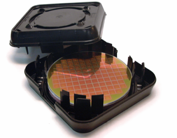
Three properties set GaN apart. GaN substrates carry a different mechanical profile than silicon, with higher density, brittleness, wafer bow, and edge-chipping sensitivity that raise bending moments at the support points and shift the failure mode from clean fracture to chipping at the contact interfaces. GaN substrates are also direction-sensitive: SiC fractures along defined crystal planes, bulk GaN cleaves under edge loading, and GaN-on-Si introduces wafer bow from the lattice-mismatched epi stack. And the active device layer sits exposed on the front side, so HEMT gates, metallization, and Schottky contacts cannot tolerate top-down clamping, abrasion, or sub-micron particulate contamination. Carriers built for silicon routinely deflect, mark, or crack GaN substrates during routine inter-fab moves.
One substrate type is not enough. The three GaN substrate variants (bulk GaN, GaN-on-Si, and GaN-on-SiC) each push handling design in a different direction. Bulk GaN ships in small diameters (50mm–100mm) and concentrates on cleavage protection. GaN-on-Si scales to 300mm and emphasizes bow tolerance plus mass-rated supports for power-device flows. GaN-on-SiC sits in between on diameter but demands the most aggressive contamination control for RF device fabs. A single carrier geometry cannot cover all three; the eGaN line provides distinct configurations per substrate type, sharing material specs and traceability standards but tuning the mechanical interface to the wafer at hand.
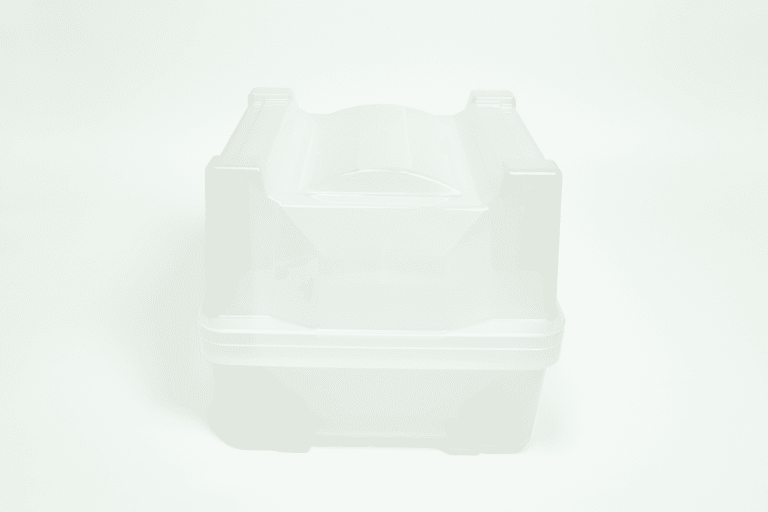
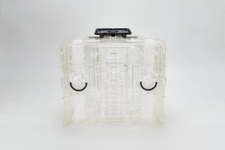
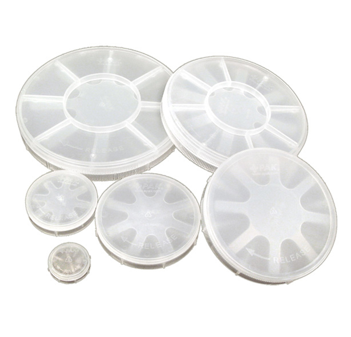
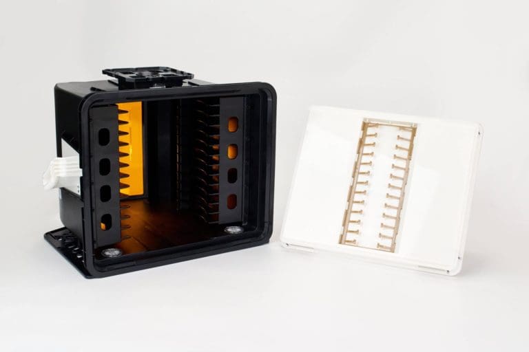
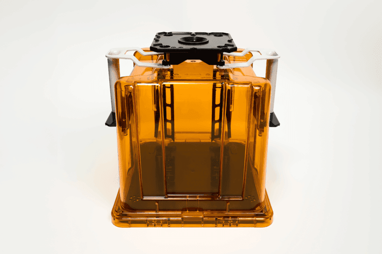
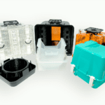
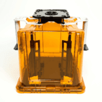
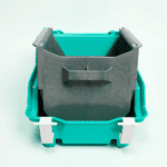
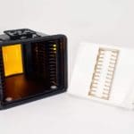
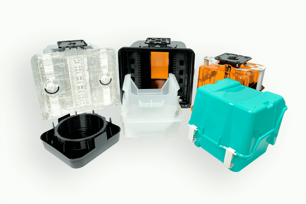
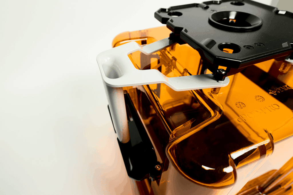
How the eGaN line is built. Every carrier in the eGaN family (the eLX zero-movement canister, the eJR wafer jar, the eFOSB front-open shipping box, the ePRO outer enclosure, the Single Wafer Shipper, and the custom engineering track) is designed against this constraint set rather than retrofitted from a silicon predecessor. Wafer supports are mass-rated, contact zones are edge or back-side, materials are static-dissipative and low-outgassing, and every product cross-references against SEMI, ISTA, and IEC standards so it integrates directly into existing fab automation. The result is a coordinated solution line built specifically for the substrates the GaN industry actually ships today.