5000 Products
500 Customers
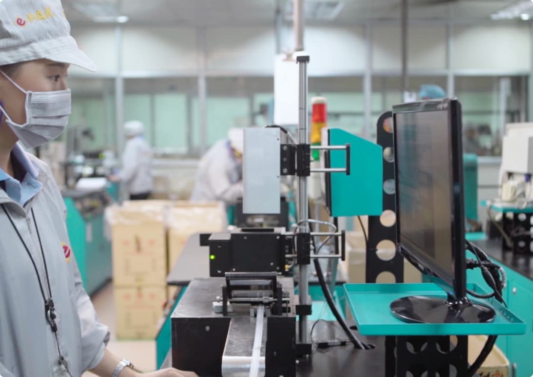
About ePAK
Founded in 1999, ePAK is a global leader in precision-engineered packaging solutions for the semiconductor industry. We design and manufacture products for front-end wafer handling, back-end IC transport, and sub-assembly handling. Our customers include top-tier semiconductor fabs, OEMs, and test and assembly houses worldwide. With a global support network and state-of-the-art manufacturing in Shenzhen and Anhui, China, and Penang, Malaysia, ePAK delivers quality, reliability, and service at scale.
ePAK’s executive team is positioned in key locations around the globe and we maintain nine sales and applications engineering offices worldwide supported by our world class manufacturing and design center in Shenzhen, China.
ePAK Advantages
Our Goal is to Provide our worldwide customers with excellent service, products and support.


Our Markets
With strong relationships built among a cadre of blue chip customers, ePAK strategically addresses a market that has demonstrated consistent global growth. Our diversified client base of more than 500 customers includes wafer fabs and assembly as well as test vendors. By establishing a world class manufacturing center in centrally located Shenzhen, PRC, we are ideally positioned to provide exceptional service and on-time delivery to our customers.
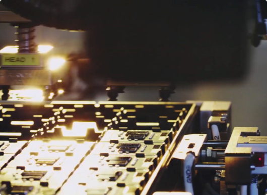
Front-End Products
Our front-end products facilitate the automated manufacture, transport and processing of semiconductor wafers while offering a high level of mechanical and physical protection. Front-end products include transport and handling carriers, process cassettes used in the manufacture of semiconductor wafers, and storage environments used for holding finished wafers and work-in-progress ("WIP") wafers.
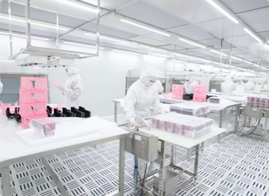
Back-End Products
Our Back-end products facilitate the handling and transfer of finished wafers, the manufacture of packaged ICs, the transport of finished ICs and electronic components to system sub-assembly and final assembly manufacturers. Maintaining the physical and functional integrity of finished wafers, fragile ICs and other electronic components is crucial to ensuring the proper operation and functionality of electronic systems.
The ability of our back-end products to reliably and consistently interface with high speed automated assembly and SMT equipment enhances high production throughput and manufacturing efficiencies.
End Systems
Our end-system products facilitate the automated assembly of electronics end systems, including magnetic disk drives for computer and consumer applications and imaging products. Sensitivity to ionic, chemical and particulate contamination is high in these applications. End-system products include disk substrate and media carriers and automation trays.

Our Executive Team
ePAK’s core management team consists of semiconductor industry veterans that have been working together for more than 15 years.


Get In Touch
If you would like to find out more about our services or one of our products, please find your nearest office and reach out
Copyright © 2026 ePAK International, Inc. All Rights Reserved.