eSiC: Silicon Carbide Wafer Handling
Ensuring Reliability in High-Performance Silicon Carbide Applications
Introduction to eSiC Wafer Handling Solutions
As silicon carbide (SiC) technology continues to drive advancements in high-temperature and high-frequency devices, ePAK’s eSiC wafer handling solutions offer critical protection and precise handling for silicon carbide wafers in applications such as power electronics, renewable energy systems, and electric vehicles.
Our eSiC solutions are meticulously engineered for SiC wafers, offering advanced protection against surface defects, contamination, and physical stress. This ensures greater efficiency and superior performance in the semiconductor industry and enhances the reliability of SiC-based devices in demanding conditions.
As a material, silicon carbide is valued for its high-temperature resilience, excellent thermal conductivity, and robust structural integrity. However, SiC wafers also require careful handling to avoid damage during manufacturing and transport stages.
ePAK’s eSiC solutions offer tailored protection to meet these needs, enabling safer, contamination-free handling across each stage of silicon carbide wafer processing. Our comprehensive solutions support SiC production from boule growth to wafer dicing and final packaging.
Download Catalog Contact UsComprehensive Solutions for Each Production Stage
1. Boule Storage and Shipping
The first step in handling silicon carbide wafers involves preserving the structural integrity of SiC substrates during boule storage and shipping. Proper containment in this stage is essential to protect crystal structure and prevent surface roughness from developing. ePAK’s solutions for boule storage are designed to protect large silicon carbide boules during growth and cooling, ensuring they remain uncontaminated and structurally sound for subsequent processing stages. Our Wafer Jars provide robust containment, featuring anti-static and contamination control properties. This combination ensures SiC wafers are handled in an environment that mitigates the risks of particle contamination. For more specialized storage needs, eLX Jars are engineered from static-dissipative polymers. These jars are ideal for high-temperature environments, where stability and resilience are required.2. Wafering and Raw Wafer Shipping
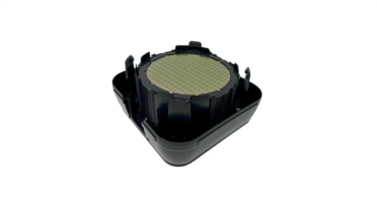
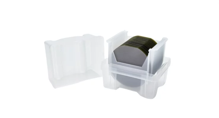
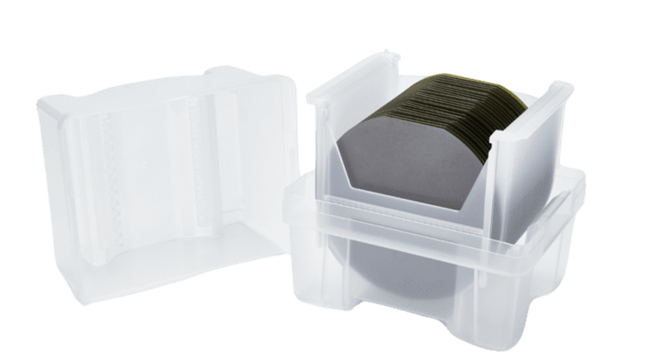
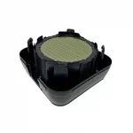
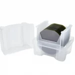
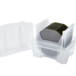
The wafering stage is where SiC wafers are sliced, cleaned, and packaged for initial transport. This stage involves handling raw wafers, which are highly susceptible to surface defects and contamination during transit. ePAK’s ePRO Raw Wafer Shipping Boxes are designed to securely transport raw silicon carbide wafers by offering dual-row cushioning for enhanced impact absorption. These boxes are built to withstand high voltage and high temperature applications, providing a reliable solution for protecting SiC wafers as they move between production stages. Our overPAKs add an extra layer of protection, making them suitable for long-distance transport in harsh conditions where environmental control is crucial to wafer integrity.3. Epitaxial Growth and Device Fabrication
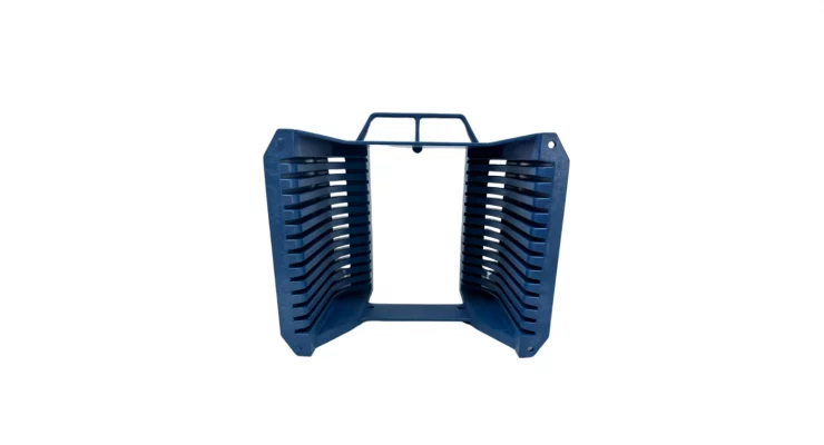
The epitaxial growth phase is one of the most critical stages in silicon carbide wafer production. This process involves adding layers of silicon carbide to create high-performance devices tailored for demanding applications. For 150mm and 200mm cassette applications, ePAK provides the ePOD PRO SMIF pod wafer carrier, a sealed, purgeable carrier with integrated N₂ purge ports for cleanroom storage and automated wafer transfer. Its bottom-opening SMIF-style interface and optional RFID support integration with compatible load ports and automated material handling workflows. Our Process Cassettes are crafted from low-shedding materials, which minimize particle generation and enhance handling efficiency, enabling precise and contamination-free SiC wafer processing.4. Shipping of Processed Wafers
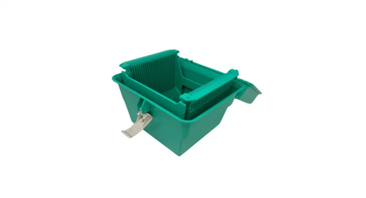
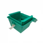
Once wafers are processed, they need secure transport to dicing and packaging facilities. ePAK’s solutions ensure that high-value silicon carbide wafers retain their superior performance and structural integrity during transit. The eLX Canisters feature ring separators that prevent wafer-to-wafer contact, which is essential for maintaining surface roughness and ensuring long-term device reliability. For flexible transport needs, our Vertical/Horizontal Frame Shippers are customizable for both vertical and horizontal orientations. These solutions are ideal for thick wafer layers, providing a tailored solution for semiconductor technology requirements.5. Wafer Dicing and Packaging
Dicing and packaging are the final steps in silicon carbide wafer handling, where wafers are cut and packed into devices. This phase requires structural support to prevent damage while allowing efficient handling. Our Plastic and Metal Frames, Hoop Rings deliver structural stability and contamination control, essential for precise, high-speed dicing operations. To support packaging, JEDEC Trays and Tape & Reel offer standardized solutions for contamination-free handling of SiC wafers in applications spanning defense industries, electric vehicles, and renewable energy sectors.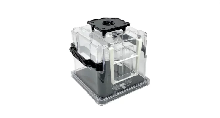




eSiC Specifications
- Enhanced Protection for Silicon Carbide Wafers
eSiC solutions are specifically engineered to offer comprehensive protection, including cushioning, shock absorption, and contamination control. This is essential for handling SiC wafers in harsh conditions without risking damage to their sensitive structure. - Contamination Control and Thermal Management
Using specialized materials with low particle emissions and static dissipation, our eSiC solutions maintain desired electrical properties and high thermal conductivity crucial for device integrity and performance. This ensures that SiC wafers can meet strict quality standards in semiconductor applications. - Adaptable for Various Silicon Carbide Wafer Sizes
eSiC solutions are adaptable to various wafer sizes, accommodating the full range of silicon carbide wafer dimensions commonly used in semiconductor manufacturing. Our solutions also integrate seamlessly with automated systems, supporting scalability in production.
Why Choose eSiC Solutions
Our eSiC solutions offer several unique advantages that enhance SiC wafer handling and processing, contributing to higher yield and device reliability.- Engineered Specifically for Silicon Carbide Substrates
Each eSiC product is tailored for silicon carbide wafers, built to endure high voltages and high-temperature environments while minimizing surface defects and contamination risks. - Enhanced Yield and Efficiency
By employing low-shedding materials and innovative shock absorption designs, eSiC solutions enhance device performance and yield, which are crucial for silicon carbide wafer handling in the semiconductor industry. - Scalable for High-Performance SiC Wafers
Our solutions are highly adaptable to various SiC wafer sizes and semiconductor applications, making them ideal for evolving silicon carbide wafer technology and high frequency devices. - Advanced Thermal and Electrical Management
eSiC solutions deliver exceptional thermal conductivity and high electron mobility, providing consistent protection in harsh environments where high temperatures and high frequency operation are necessary.
Technical Specifications
Each product in the eSiC line is developed with specific technical specifications to ensure compatibility with silicon carbide wafer handling requirements. Our products feature static-dissipative engineered polymers, which prevent particle emission and maintain a high level of cleanliness during wafer handling and transport. Hermetically sealed designs and low-shedding materials protect SiC substrates in extreme temperature environments, supporting contamination control. Dual-row isolated cushions in our ePRO boxes and ring separators in eLX canisters protect SiC wafers from physical damage, ensuring reliable performance throughout each handling stage.Frequently asked questions
What makes eSiC solutions ideal for silicon carbide wafers?
Can eSiC products handle both 4H-SiC and 6H-SiC wafers?
How do eSiC solutions support electric vehicles and 5G applications?
What contamination control features are included in eSiC products?
Can eSiC products be customized for specific production needs?
How does eSiC improve yield in SiC wafer production?
Wafer Shipping & Handling Catalog
Our catalog covers a wide range of products specifically tailored to handling your wafers. Please contact us if you need custom solutions to your projects.