What Indium Phosphide Asks of a Carrier
InP wafers are brittle, small in diameter and high in value, and their device side is easily degraded. These properties drive the design of ePAK's InP carriers.
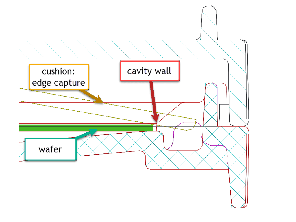
Brittle by nature. Fracture toughness well below silicon. InP cleaves readily along crystal planes: a point load or edge knock that silicon withstands can shatter it. Our answer: edge-only capture, recessed seats and constrained movement in transit.
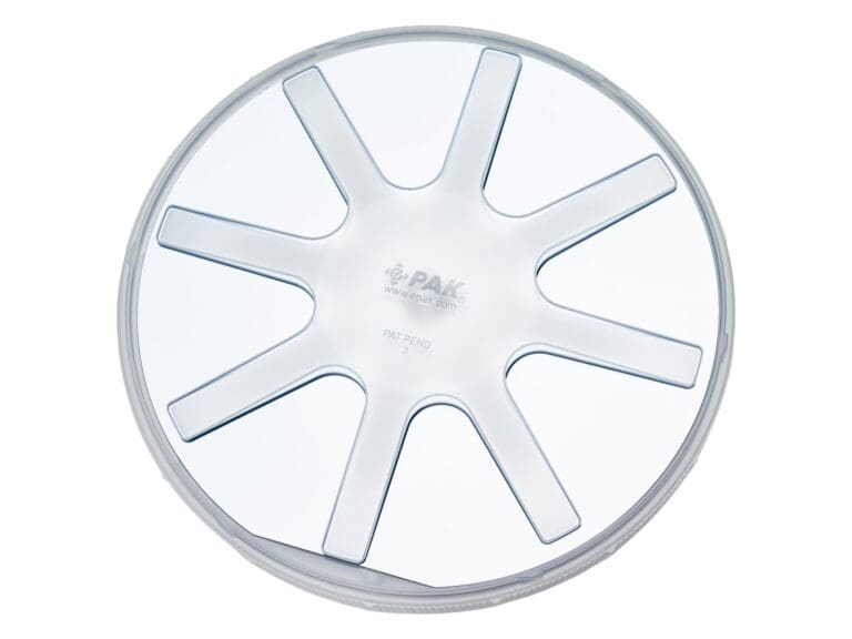
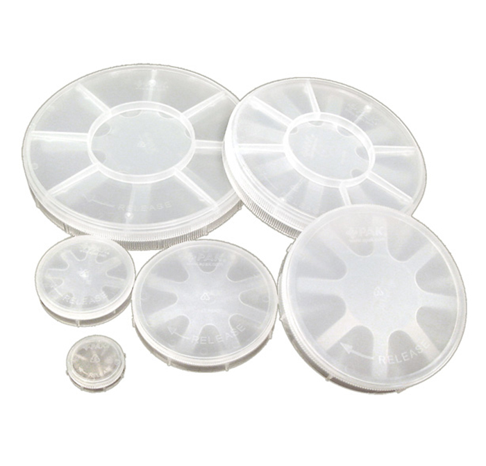
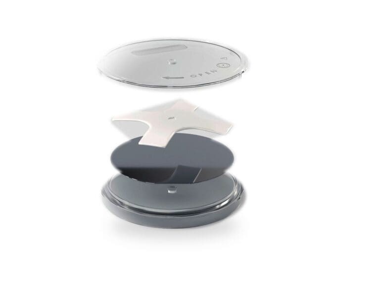
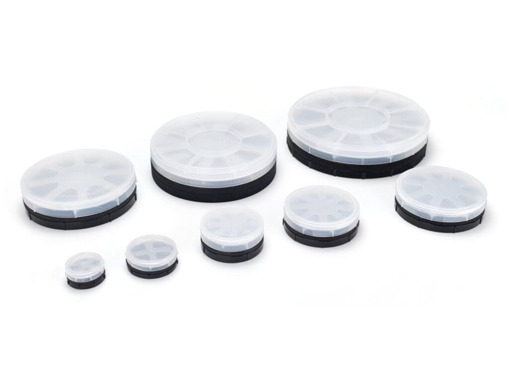
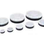
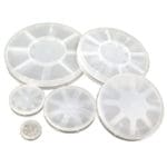
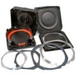
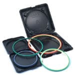
Small diameters, high value. InP wafers run from 50mm to 150mm in diameter, and each wafer carries high value. One broken wafer inside a multi-wafer shipper can ruin the entire lot. Our answer: single wafer coin shippers that protect one high-value wafer at a time.
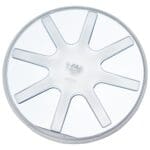
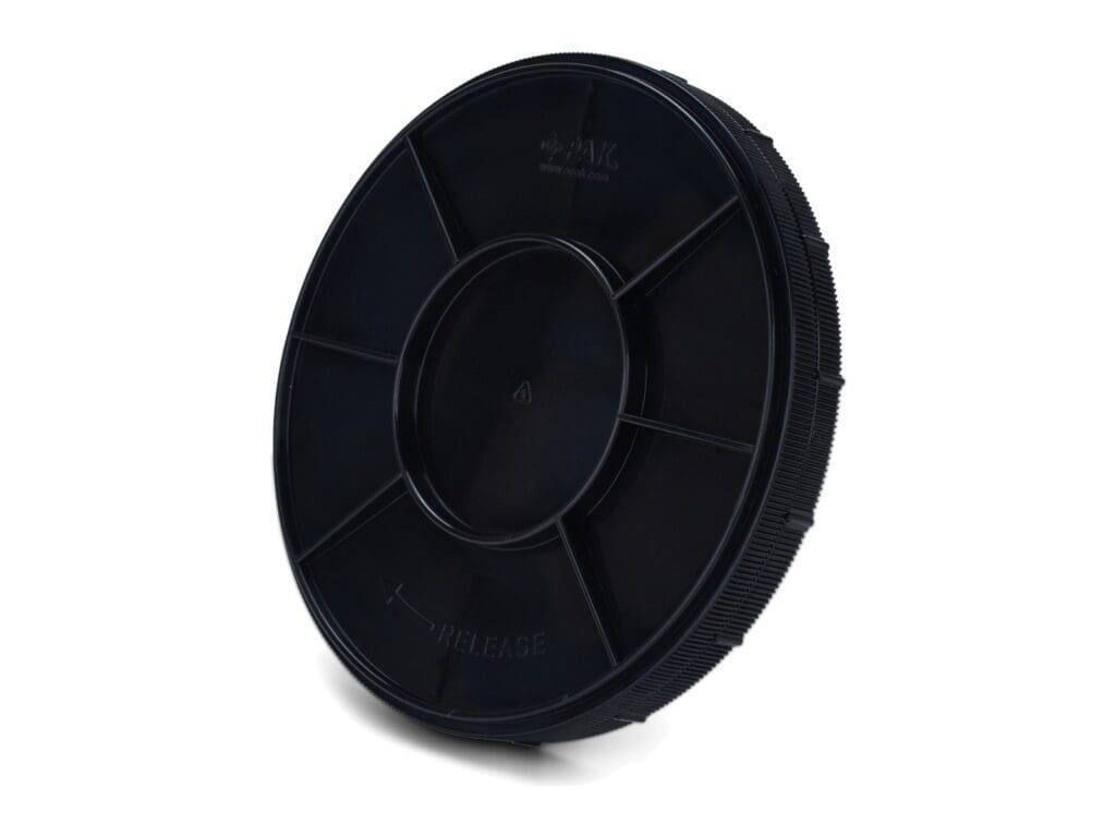
Mirror-finish device side. Particles, outgassing residues or ESD degrade laser facets and detector responsivity, and damage is often invisible until wafer-level test. Our answer: the 150mm coin shipper holds the wafer by its outside edge only, with no contact on the wafer surface, and conductive PP (10⁴–10⁵ Ω/sq) is available as a material option.